CIRCUIT
DESIGN
2. Packaging
3. Circuit Design
3.1 General
3.2 Toggle
3.3 Nor
3.4 Pulse gate
4. Conclusion
Acknowledgements
2. Packaging
3. Circuit Design
3.1 General
3.2 Toggle
3.3 Nor
3.4 Pulse gate
4. Conclusion
Acknowledgements
by F.G. Heath
(Issue 1 - August 1963 EP 54)
Ferranti Ltd., 1963.
Computer Technical Services Department
Orion 2 and FP6000, like such previous Ferranti machines as Argus, Poseidon and Gemini, use NOR logic with Eccles-Jordan toggle circuits and a special type of pulse gate. The most versatile version so far designed is that for Gemini, and this family has been adopted, with minor modifications, for Orion 2 and the Gorton-built FP6000.
The system sacrifices some of the inherent component speed at the outset of the design in order that a simple set of loading rules may be available to the logic designers. The system is insensitive to internal race conditions and the consequent short pulses or snigs, and approaches the theoretical best performance against external noise for any given computer clock frequency.
The simplicity of design which can be achieved by this method, coupled with the reliability which comes from a well-covered set of loading rules is normally sufficient compensation for some loss of operating speed, which may in fact be more apparent than real if the alternative design takes care of worst-case race conditions.
This note will use B.S.I. graphical symbols (Supplement 5 (1962) to B.S. 530) and terms (B.S. 3527 : 1962) except in production circuit diagrams which were prepared before the standard. The term flip-flop is used as well as toggle because of its popularity within Ferranti. Detailed calculations will not be given in order to help continuity, but a Mullard report on the basic circuits is included as Appendix 1.
It is well known that any logic design whatsoever can be set up using ‘and’, ‘or’ and ‘not’ elements alone, and that any two of these are adequate if the input signals can be specified by the designer. Since the ‘not’ function is conveniently combined with the non-digital but necessary operation of restandardising the levels, the usual two-element combinations are ‘and-not’ (NAND) and ‘or-not’ (NOR). The duality laws mean that these two may be regarded as the same thing, since a change of 0 & 1 definition inverts the cases.
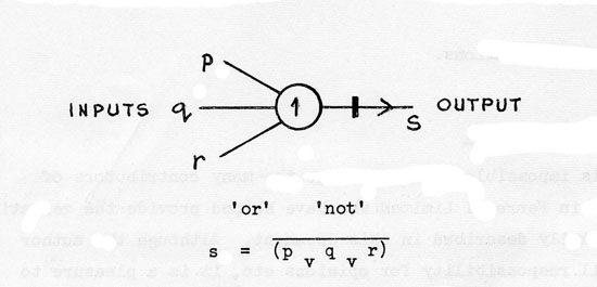
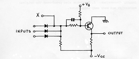
A general name for the common circuit is ‘single level diode logic and invert’. If 0 is defined as the collector voltage of a cut-off transistor and 1 as the collector voltage of a saturated transistor, then the simple case becomes an ‘or’ gate + inversion, and within Ferranti is termed a ‘nor’ circuit. Figure 1 shows the logic symbol, and Figure 2 the circuit diagram.
Only if all three diodes are connected to logical 0 inputs can the transistor in Figure 2 conduct, which gives logical 1 at its output, the definition of ‘nor’.
The virtues of this circuit lie in its high fan-in and fan-out values, which may be relatively easily calculated from worst-case a.c. and d.c. characteristics of the components. It is also economical of components, the speed relationship working out so that for any given speed of operation the diodes can be made by a cheap technology compared with the transistors.
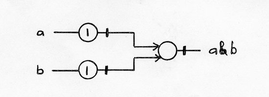
The ‘not’ operation can be obtained by using elements with only one input connected, so that ‘and’ can be generated as shown in Figure 3, but to apply this as a general rule would be wasteful. It is obvious that a circuit giving both normal and inverse outputs is desirable, and this has been attained by using as register elements the Eccles-Jordan toggle circuit.
The basic toggle circuit may be used in several different ways however, three of which are described here. The basic circuit is equivalent to a pair of cross-connected ‘nor’ elements, and may be termed a logic toggle. This circuit will set or reset at any time when a voltage pulse greater than some minimum amplitude and exceeding a minimum duration (the toggle resolution time) is applied to the appropriate input.
Ideally any two signals in the same machine epoch should have identical time profiles, but in practice due to differing circuit performance and wire-lengths this is not so. Consequently any two signals which are gated together will generate at some time a short spurious pulse which may trigger a toggle.
This can be termed a type 1 race condition, and may show itself in a previously satisfactory machine if improved transistors become available which reduce the toggle resolution time. This effect can make machine behaviour most erratic.
The solution to this difficulty is to strobe inputs to the toggle circuit, so that set and reset only take place at times which are defined by a separate circuit. This strobing can be done via a normal logical connection as in Atlas, but in the family of Ferranti machines which use the principles described here, the timing waveform has a special connection and the logic inputs are fed through integrating circuits.
This arrangement overcomes the type 1 race condition, and also makes sure that a very fast logic edge fed to a very fast toggle does not set (or reset) the circuit one strobe pulse ahead of the designers intention, (a type 2 race condition).
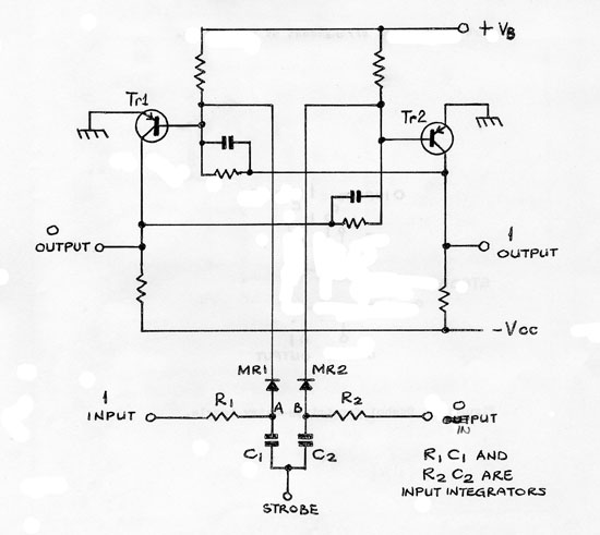
The input circuit may be considered to be a noisy binary channel, with extraneous noise impressed asynchronously. Obviously the circuit will be least affected by this type of noise when the input RC time-constant is so large that the computer can only just work at its design speed. Figure 4 shows the logic symbol and Figure 5 the simplest circuit diagram for an Eccles-Jordan toggle circuit with separate strobe terminal and input integrators (which serve also as transient memory). For brevity this type of circuit will be referred to simply as a toggle from this point.
The logic input signals must have enough time to charge C1 and C2 adequately before the strobe pulse is applied. The strobe pulse duration is governed by circuit and transistor parameters, and must therefore be controlled.
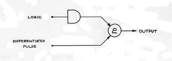
There must be fairly tight limits on rise and fall time and the load is capacitive, so that the simple ‘nor’ circuit cannot be used for timing purposes. A special circuit, the pulse gate, is designed for this task, and its logical operation is that of ‘and’. Type 2 race problems make an integrator or delay necessary in the logic input, so that a composite logic symbol for the pulse gate could be drawn as in Figure 6.
The three elements, nor, toggle and pulse gate are theoretically adequate for constructing the central processing unit of a computer, but designers admit two others for reasons of economy, triple entry toggle and power nor.
It is often useful to have more entries to a toggle than just the one shown in Figure 5, and by duplicating R1, R2, C1, C2, MR1 and MR2 a double-entry toggle can be obtained. Early experience with Argus indicated that a triple entry version is needed, and that little wastage occurred by using triple entry circuits in double-entry applications.
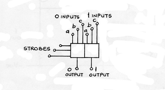
A similar circuit used in Orion 2, has 6 inputs and three separate strobe lines, and the symbol is shown in Figure 7.
Another discovery in the early Argus work which has proved generally useful is that a percentage of ‘nor’ stages has to drive more circuits than is possible with low-power transistors. Instead of using a single uneconomic powerful ‘nor’ stage for both purposes, or designing an emitter-follower package, it was found better to have a power-nor circuit for the special cases. This choice was adopted in Orion 2.
This affects the circuit principles slightly, and is worth describing, since the Gemini methods overcome the problem of constructing a machine economically from a small number of package types. Argus is limited by the number of socket outlets on a package, so that many rearrangements of the same basic circuit are needed.
The Orion 2 package has double-sided printing and uses a 22-way double-sided connector so that 44 ways are available into a fairly small printed board. Consequently, if a number of ‘nor’ circuits are packed on a board, there are pins available to bring out the common entry point of the ‘nors’ (point X in Figure 2) and pins are available on the standard package types for spare logic diodes, which may be connected to point X when required. Thus a single ‘nor’ package may be used in a most versatile way by using the back-wiring to build up multi-input gates.
An additional feature possible because of the greater number of pin connections is that of common collector ‘OR’ing. This requires that the collectors of the inverting transistors are connected together directly with the omission of one or more of the load resistors. This is provided for by having all collectors brought out to separate pins for their load resistors, interconnection being via the box wiring.
The circuit diagram of the standard ‘nor’ package, the 701, is shown in Figure 8. Figures 9, 10, 11 and 12 show circuit diagrams of the single entry toggle, pulse gate, triple-entry toggle and power ‘nor’ respectively.
This section shows how the d.c. and a.c. design of the various circuits yields the loading rules, noise sensitivity and maximum clock speed of a computer using them. Detailed calculations will be found in Appendix 1. Factors which need evaluation are:-
1. Fan-out
2. Set/reset time
3. Noise sensitivity
1. Fan-in
2. Fan-out
3. Propagation time
4. Noise sensitivity
1. Fan-in
2. Fan-out
3. Delay time (must be consistent, rather than short)
4. Noise sensitivity
The triple entry toggle and power ‘nor’ involve no fresh principles.
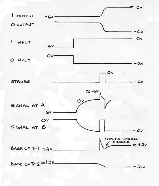
If the simple toggle circuit of Figure 5 is operated, the waveforms when setting will be found to be as in Figure 13. The input signals (both of them) must have enough time to charge C1 and C2 before the strobe pulse is applied. The charged capacitor (C1 here) lifts point A up to nearly +6V in theory, but only a thin spike is visible, since the transistor is a heavy load. However this low impedance circuit sweeps the stored charge out of the base region of the transistor with maximum speed, and C1 must be large enough to extract all the holes without being completely discharged at the end of the shift pulse.
Provided the collector of the turned-off device has passed the balance point of the circuit at the end of the shift pulse, then the Eccles-Jordan connection will complete the switching operation.
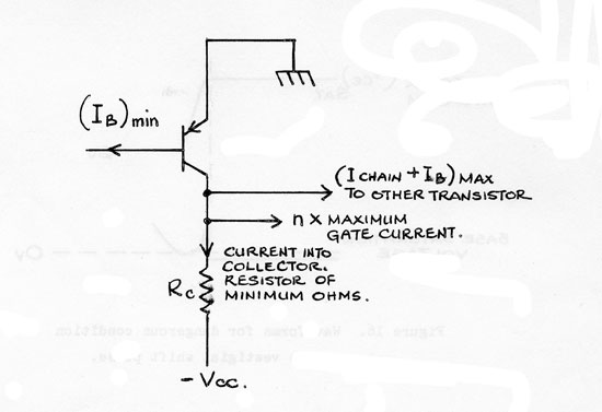
The d.c. fan-out of the circuit is determined by the number of ‘nor’ diodes which can be connected to the collectors before the operating margins become so slender that component or power supply tolerances are spoiled. Figure 14 shows the loading on a turned-on transistor, which must not leave the saturation region.
Obviously the fan-out is limited by (IB)min multiplied by the minimum bottomed current gain of the transistor, and the stated value of 5 is comfortably covered.
A toggle circuit is best designed to switch as rapidly as possible without selecting components or spoiling the d.c. design. Transistor parameters which determine how soon the transistor is turned off are hole storage (in the base region normally, but sometimes in the collector) and base spreading resistance. The speed with which the collector then reaches the changeover point is determined by collector capacitance and wiring capacitance.
If the resultant computer is to be fast, then shift pulse duration should be related to hole storage and base spreading resistance only, the circuit capacitance being controlled by a loading rule. The input capacitors can be related to stored charge alone, on a worst case basis. The calculations are not quite as simple as this at the highest speeds, but the principles still hold, and it is possible to give the transistor manufacturer a clear picture of what is needed in the devices.
The shift pulse duration for the Orion 2 machine is 0.3 μs (0.15 µs rise and fall times. Worst case under full output load condition) which is generously more than worst case for switching ASZ 21 transistors with 200 pF capacitors.
The resistor which charges the capacitor must be chosen so that the toggle which drives it only has to supply a reasonably low transient current otherwise switching might not occur. The Orion 2 circuits use 470 Ω, which gives a time-constant of 94 ns in the integrating circuit, so that the transient load has approximately three time-constants to die away before the end of the shift pulse, and previous stages can switch reliably.
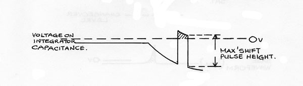
It is possible to calculate the length of time after switching the input signals before it is safe to apply the shift pulse. The input which can cause faulty operation is the negative-going edge and is shown in Figure 15. The shaded area might just switch a very fast transistor. In practise three time constants is sufficient to allow for this purpose, so that the minimum set/reset time is 3RC + TP
= (3 x 0.094 + 0.3) μs
= 0.58 μs.
There are usually three types of noise to be allowed for in computer design, which may or may not give rise to similar effects depending on the individual machine design. The method of correction is very different in each case however.
The first type may be termed external noise, even though it is frequently generated by peripheral contacts, drum motors etc. The amplitude and epoch of such noise is not related to any machine waveform, and can be controlled by isolation, smoothing and screening techniques. The final form of such signals inside the machine ought to be small rounded pulses occurring at random times.
Internally generated noise on the other hand is produced within the machine logic circuits by racing conditions, as previously described. Consequently the techniques which remove external noise cannot be applied (except that the input integrators in this case improve signal/noise ratio somewhat) and suppression methods which rely on time-relationships must be employed, such as the strobing techniques described in section 1.
A third type of noise is also internally generated, but finds its way into other circuits via ohmic or inductive coupling in earth leads or by simple electrostatic pick-up. Methods suitable for external and internal noise can be applied here.
For the toggle circuit considered here, noise may enter through the input terminals or the strobe line. It is convenient to calculate effects by applying standard inputs and then measuring the amplitude of shift pulse which will
(a) Switch the circuit when it should not:
(b) Not switch the circuit when it should.
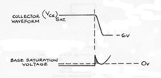
Condition (a) depends on the fastest transistor which is included in the specification, and it is rare to find a manufacturer who takes seriously a complaint that his transistors are too fast. Figure 16 shows the base waveform, and if the shaded area can just switch the fastest transistor, then the amplitude of shift-pulse may be defined as the noise susceptibility for one polarity.
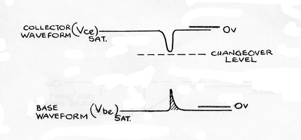
Condition (b) depends on the slowest transistor, which is usually controlled much more carefully, so that this side of the characteristic can be calculated. Figure 17 shows the base and collector waveforms, and the amplitude of shift pulse which just does not shift the slowest transistor may be subtracted from the normal shift-pulse to get the noise susceptibility for the other polarity.
In practise both these voltages are worth measuring on a percentage of packages, since they give a good quality control of components. Figures for the Orion 2 single entry toggle circuit are:-
Max. size to give effect as Fig. 16 (Switching when
not intended) 1.5V
Min. size to give effect as Fig. 17 (Not switching when intended) 4.5V
For a gating element the loading rules can be considered in two parts, d.c. and a.c. Normally it is possible to design the d.c. loading rules round worst case component parameters without too much loss of performance, and this has been done in this case. For a.c. parameters the situation depends on the machine logical design. If (as in Orion 2) a maximum of ten gates in series is allowed between toggles, then it is realistic to put a statistical control on delay time etc, since the chance of getting ten worst case gates in one chain is far less than the number of computers one is liable to make. On the other hand if only one gating operation is performed between toggles then the a.c. gate properties should be controlled by worst-case methods.
The d.c. limit of fan-in is of little practical importance, since it occurs, in general, well after the a.c. limit of fan-in has been reached. If n diodes are connected to a standard nor circuit, with (n-l) anodes at -6V approximately, then when the ‘on’ diode anode goes to -6V, the circuit resistance has to charge up all the usual capacitances plus (n-l) x diode depletion capacitance. This is aided by the stored charge of the ‘on’ diode.
The Orion 2 circuits limit fan-in to 17 and one diode switching against 16 worst-case diodes gives a stage delay of 24 ns.
The considerations here are the same as for the toggle circuit, in that fan-out is determined by the number of diode loads which can be connected to a worst case bottomed transistor without it leaving the saturation region.
In the Orion 2 circuits the minimum d.c. current into the base of a turned-on transistor is 0.65 mA. Multiplied by 33, the end-of-life hFE this gives a worst-case collector current of 21.5 mA. The collector load takes 6 mA of this, leaving 15.5 mA for diode loads into toggles at 2.4 mA each. This gives good worst-case cover for three loads.
It is possible to treat the d.c. designs of these circuits worst case without losing a lot of performance. The same is not true of the a.c. design, since to make each of ten gates, all in series, worst-case would be to slow down the computer unreasonably. Thus the testing and specifying of a.c. properties ought to be statistical, and the Mullard calculations and measurements, recognising this, give typical values.
Key parameters in the a.c. design are the hole-storage etc. of the transistor, and the maximum wiring capacitance which may be connected to a collector. These values determine (in conjunction with shift pulse data) the possible values for the speed-up capacitances and the input capacitances C1 and C2 of Figure 4.
If these capacitances are too small, then ‘nor’ stages slow-down by a large factor, and toggles fail to switch. Both these effects can be catastrophic. If the capacitances are high, then the only penalty may be a slight reduction in clock rate in order to charge up the input capacitances, which is a small price to pay. The ideal solution is to keep close control of the charge parameters of the transistors, and possibly wire-lengths in boxes.
The worst case setting time of the toggle (section 3.2.2) is 0.58 μs. Orion 2 design principles allow a maximum of ten gates in series. The typical gate delay with worst case loading is about 20 ns, and an estimate of σ for this delay is 4 ns (per package).
Over 10 packages, σ = 4/√10 = 1.25 ns,
so that allowing 4σ limits on the chain gives a 10 gate maximum delay of 10 x (20 + 4 x 1.25) ns = 250 ns.
Therefore computer clock time = (0.58 + 0.25) μs = 0.83 μs.
Therefore worst case maximum clock frequency = 1.2 Mc/s.
The main noise problem with the basic nor circuit arises if the diodes which perform the input gating are turned slightly on when all inputs are at -6v by the effect of adverse tolerances or design in the resistor chain to -28V.
This effect was calculated to be possible for worst-case circuits designed as table 3 in Appendix 1, and for this reason (as well as the speed disadvantage) this design was eliminated.
It will be noted from Appendix 1 that Mullard cannot recommend the Gemini pulse gate (because of the risk of damage in commissioning) but present no alternative. Experience shows that in a diode pump machine the circuit which charges the switching capacitors rapidly must be a high-current low impedance source, and the risk must be accepted. The circuit has the great virtue of being a clamp both ways.
Figure 10 shows the circuit of the pulse gate. C1 is charged (or not) from an input diode, so that when a shift pulse arrives on 11R Tr1 turns off (or is uncharged).
If C1 was charged by a logic 1, Tr1 turns off, Tr2 turns on and the complementary output pair give a shift pulse. The shift pulse duration is determined by the input pulse duration if less than 0.3 μs. Alternatively, the differentiating effect of C1 R2 keeps the output pulse duration to 0.3 μS. No regenerative timing effect is available, so that the circuit is calculably sensitive to input noise at all times, never exhibiting any kind of paralysis.
Since the logic inputs are driving an integrator, the fan-in limits are extremely tolerant, and calculation is rather pointless. The circuit has the ‘or’ point brought out, so that no mechanical fan-in limitation is present.
The output of the pulse-gate is heavily loaded if every stage it supplies is switching, so that the fan-out must be rigidly controlled. The d.c. design uses a considerable excess of current gain through the circuit in order to achieve speed, and a valuable criterion is the maximum output current. In this case 150 mA is reasonable (devices rated at 200 mA) and the fan-out of 10 with maximum switching means that 2,000 pF must be discharged in 0.3 μs.
Therefore CV = 12 x 10-9 coulombs = 120 mA for 0.1 μs. The ‘d.c.’ fan-out is therefore covered.
In a synchronous machine using the design philosophy outlined earlier, it is a very sound precaution to design so that every pulse gate output used by a toggle is generated via the same number of delays down timing waveform inputs.
This has been done in the Orion 2, so that delay time difficulties in the shift gate will only show up due to excessive spread rather than absolute value of delay. Although no standard deviation (σ) measurements were made, the Mullard typical value of 30 ns indicates a probable σ of 5 or 6 ns, which should not lead to timing troubles.
It was mentioned earlier that the pulse gate used in the Orion 2 machine has no "snap" action. Consequently at any time it is possible to calculate an amplitude of pulse which will break through the input circuit, and towards the end of the timing waveform the circuit is quite sensitive, so that ringing inputs may cause thin output pulses which can trigger fast bistables.
This limits the use of the circuit on long lines, and has been detected in practice. Once the designer is aware of the effect its calculation in any particular case is straight-forward.
The central circuits of the Orion 2 machine as proposed for production have been described, and the various effects outlined. It has been shown that the maximum clock rate is 1.2 Mc/s, from worst-case calculations
It is impossible to acknowledge the many contributors of ideas within Ferranti Limited who have helped provide the versatile package family described in this document. Although the author takes full responsibility for opinions etc, it is a pleasure to record the help provided by P.S. Levis and J. Templeton during lengthy discussions. J. Templeton also proof-read the original manuscript made many suggestions.