2. Packaging
3. Circuit Design
3.1 General
3.2 Toggle
3.3 Nor
3.4 Pulse gate
4. Conclusion
5. Ack'ments
Appendix 1
2. Packaging
3. Circuit Design
3.1 General
3.2 Toggle
3.3 Nor
3.4 Pulse gate
4. Conclusion
5. Ack'ments
Appendix 1
Summary: This new computer uses Base Current Switched Logic with R.C.A. diodes and transistors. These are the IN54A and 2N393. This investigation was to find what circuitry changes were required to make use of the OA47 and ASZ21.
Author: P. James
Date: 3rd December, 1962
The range of Ferranti packages considered were designed in Canada using
semiconductors available there. Ferranti were interested in using Mullard
semiconductors for three of the basic circuits, the NOR circuit, the Bistable
and the Pulse gate circuits. This memo gives the results of the investigation.
As a computer which was going to use these packages was already designed, the circuits need to operate under the same conditions as the original circuits and so the boundary conditions are as follows.
a) The supply voltages are to be +6, -6 and -28 volts. All supplies are to be ± 5%.
b) When a transistor of the NOR circuit is on then all input diodes should be reversed biased in order to minimise noise effects.
c) Resistor tolerances should be ± 10% which was later provisionally improved ± 5%.
d) As the layout was fixed, no variations in numbers of components or their positions was allowed.
e) A worst case design should be used.
f) The speed should be no worse than using the 1N54A and 2N393 but improvements would of course be preferred.
g) The ambient temperature range is 10ºC to 55ºC.
h)
If possible the circuits should be compatible with the original circuits.
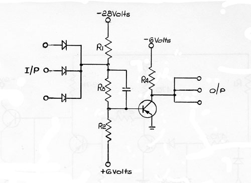
The basic NOR circuit1,2 is as shown in fig.A1. A variation of resistor values was required due to the higher bottoming voltage of the ASZ21. This was partially, compensated by the lower forward voltage drop of the OA47 over the 1N54A. The leakage current of the ASZ21 at 6V is 60 µA maximum compared with an estimated 15 µA for the 2N393.
One suggested set of values for this NOR circuit is given below.
Table 1
R1 = 10K
R2 = 6.8K
R3 = 2.2K
R4 = 1K
C = 33pF
All resistors are ± 10%
This is a worst case design allowing for IT inputs and 6 outputs simultaneously. The mean dissipation of the circuit is about 87mW as compared with 84mW for the original circuit. This increased dissipation has been accepted by Ferranti but a design using 5% tolerance resistors (also now acceptable by Ferranti) with less dissipation than the original circuitry, may, be used. The circuit is given below.
Table 2
R1 = 12K
R2 = 8.2K
R3 = 2.4K
R4 = 1K
C = 33pF
All resistors are ± 5%
The mean dissipation is 83mW.
Both circuits have been designed to have a worst case hold off voltage of 0.2 volts in order to prevent noise signals affecting the performance. The noise may be from two sources which are cross talk signals and signals due to hole storage of the logic diodes.
It is possible with 5% tolerance resistors to increase the worst case hold off voltage to 0.5 volt. This increases the delay per stage by 3n sec. and the dissipation to 95mW. The components are now as in table 3.
Table 3
R1 = 10K
R2 = 5.6K
R3 = 2.2K
R4 = 1K
C = 33pF
Only a summary of delay times is given as these are a factor of 2 better than required. More measurements would be required in order to give enough details for working nearer the limiting speed of these circuits.
Using the circuit of fig. A1 and table 1 the typical measured delays are as follows:-
|
Input Branching |
Output Branching |
Other Remarks |
Delay/stage |
|
1 |
1 |
no stray capacitance |
10 |
|
1 |
6 |
“ |
11 |
|
17 (16 unswitched) |
1 |
“ |
14 |
|
1 |
1 |
33pF on each collector |
18 |
|
1 |
1 |
no stray capacitance |
12* |
|
17 (16 unswitched) |
1 |
|
17* |
|
17 (16 unswitched) |
1 |
as above with maximum |
24* |
* These figures are only meant as a rough guide as a true worst case would be very difficult to simulate and unlikely to happen.
The measurements have been made on tag strips and a slight increase might be required due to the strays on the printed circuit boards.
The delay required for this circuit was 35nS
with no stray capacitance and so the
figures given above are well within this
limit. The 1N54A circuit has a 1 in 1 out
delay per stage of 22nS measured over
12 stages.
There are two effects due to diode hole storage which are
a) Speed up of turn on.
b) Transient turn on when a large number of input diodes are switched from conducting to reverse biased and one remains conducting.
The speed up effect of hole storage will be ignored so that the only problem as far as diode hole storage is concerned is the possibility of transient conduction. This partial switch on depends not only on the actual values of components and transistor and diode parameters but on the logical configuration and which inputs are switched.
The only places where the transient conduction
could affect the computer performance are if outputs of NOR circuits are
connected to the output of a bistable and if the circuit is working to its
limiting frequency. The former could cause incorrect switching of the bistable
but in this machine Ferranti have stated that bistables will not be switched in
this manner. The latter is not likely to arise as the limiting frequency will
not be used as in worst case design the delay allowed is much greater than
actually occurs.
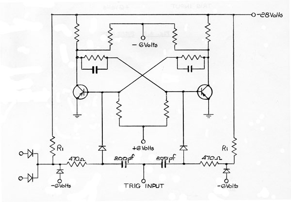
There are three forms of bistable circuit which are variations on the circuit of fig. A2 which shows the original single entry bistable. The double entry and triple entry bistables have additional single inputs and shift pulse inputs. The duplicated circuitry is shown enclosed by the dotted lines. The redesigned bistable could be two NOR circuits cross-coupled together with the steering networks and in fig. A2 this is the case.
The circuit operates with 66pF added to the
collector of each capacitor to simulate the maximum length of wire allowed from
each output (2 feet) with a delay of 100nS between the shift pulse and the rise
of the transistor switching on.
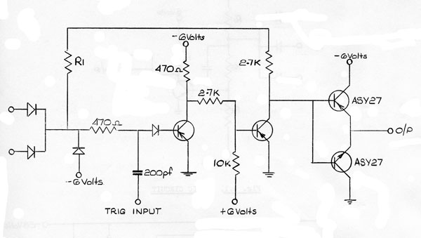
A pulse gate circuit is used to supply a shift pulse to 10 bistable circuits. It is also used as an intermediate amplifier between either the power NOR circuit (not described in this memo) and a subsequent pulse gate or between pulse gates. The circuit is shown in fig. A3. The double emitter follower output uses the N46C and N9C (ASY27 and ASY29) transistors and both the other transistors are type ASZ21.
The measured turn-on delay was 90nS but this would be improved by taking the load of the driver to the -6 Volts supply instead of the -28 Volt supply. This is because the current in the driver has to build up from zero to that value necessary to give 21 Volts across the load resistor before any current flows into the double emitter follower circuit. Using 2.7K connected to the -6 Volts supply the turn-on delay, is reduced to 30nS.
This pulse gate circuit cannot be recommended as a fault condition on the output could "blow up" the two output transistors and under normal operating conditions the peak current of 200mA could be exceeded. This did not happen with the circuits tried where the peak current was found to be 150mA.
The bistables only, require a fast rising edge to
trigger them but a suitable circuit could not be found which gave sufficiently
fast operation.
The bistable and pulse gate circuits are compatible
with the original circuits using the 1N54A and 2N393 and a NOR circuit using the
1N54A and 2N393 will drive a NOR circuit using the OA47 and ASZ21, but, under
worst case conditions, the ASZ21 NOR circuit will not drive the 2N393 circuit.
Provided that either the dissipation of the circuits may be
increased by 10% or the resistor tolerance reduced to a total excursion of 5%
then the OA47 diode and ASZ21 transistor will allow an increase in the clock
frequency, from 1Mc/s to l.2Mc/s.
1. S.M.A. Report No. 35
2. S.M.A. Report No. 51